
Grid Power Electronics
From Analog to Digital Grids
It’s intuitive to think of electric grids as inherently “digital”, since they are controlled flows of electrons just like our modern electronic devices. In fact, even today most of our electricity grids are largely analog machines. Power is generated with giant spinning turbines, and then funnelled and shaped using large lumps of metal, magnets, and insulation to reach into our homes and businesses to power our devices. The spinning motor in your washing machine spins in harmony with the spinning generator of a distant power plant, dictated by the frequency of the alternating current between them. The entire grid operates passively based on the physical properties of the materials involved, with no logic or software directly controlling them. However, a major transformation is now underway that is rapidly bringing electricity grids into the digital realm.
In the 1960’s, electronic devices were developed that could actively shape and control electric currents in much the same way as the mechanical devices on our grids, but far more efficiently and on a much smaller scale (invented at Bell Labs, naturally). These devices are collectively referred to as power electronics. One of the key building blocks of power electronics are transistors that shape the flow of a DC current by opening and closing logic gates that turn the current on or off. This in turn can be used to raise or lower voltage, or to create an alternating current from a direct current. The technical term for these building blocks are metal-oxide-semiconductor field-effect transistors (MOSFET).
While the term is a mouthful, the basic concept is very simple. You plug your laptop into an outlet that provides a 120V current, but it contains a computer chip that only needs a 1V current. The passive way to achieve this is to use magnetic transformers to step down the voltage, which are bulky and inflexible. Alternatively, one could use resistance to absorb the excess voltage, but this is extremely inefficient. Instead, a MOSFET acts as a high-speed switch, “chopping” the current thousands of times per second. By precisely controlling the time the gate is open or closed (pulse-width modulation), it can turn a 120V input current into an output current with an average voltage of 1V with very high efficiency.
While MOSFETs are now extremely common in consumer electronic devices, the first generation were made from silicon, which cannot handle grid-scale voltages. Beyond a few hundred volts, the internal structure of silicon reaches its physical limit, leading to a catastrophic breakdown where current surges through the material, destroying the device.
To overcome this voltage limitation, a second generation of grid power electronics called insulated-gate bipolar transistors (IGBT) were developed in the 1990s. An IGBT combines the digital control of a MOSFET with the high voltage capacity of a bipolar transistor. In these devices, a MOSFET is used to turn on or off a larger current that floods alternating layers of silicon with both positive and negative charges. This causes a thick piece of silicon to suddenly become highly conductive, overcoming the resistance limits that would melt a standard MOSFET. The downside is that when the switch turns off, this charge slowly dissipates as waste heat, reducing its efficiency and requiring external cooling in many cases. This tail current also puts a limit on AC frequency switching speed, so while it can operate at a higher frequency than the grid, it cannot support the very high frequency switching speed of a standard silicon MOSFET.
To briefly recap, the state of power electronics until recently was a choice between speed and power. You could have very high frequencies at low voltage (with a silicon MOSFET), or high voltage at low frequency (with an IGBT). On the grid, high voltage and low frequency translates to requiring very large transformers, since a large mass of copper and iron is needed to capture the magnetic flux without overheating. If we found a way to support much higher AC switching frequency, we could dramatically shrink the size of transformers required. At higher frequencies, the magnetic core of a transformer can transfer the same amount of energy with a fraction of the physical material.
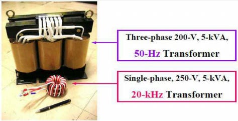
Size comparison between high frequency (20 kHz) and low frequency (50 Hz) transformers (source).
The SiC Revolution
In the past decade MOSFETS have been developed with a new material, silicon carbide (SiC), that finally escapes the speed vs power tradeoff. Silicon carbide is a semiconducting material much like pure silicon, but is a much stronger insulator when the gate is in its “off” state (in technical terms, it has a wider bandgap). This allows a MOSFET made from SiC to operate at much higher voltage, with the latest models able to handle as much as 10 kV (Wolfspeed). Groups of these SiC MOSFETs can also be brought together into modular multi-level converters (MMCs) to handle even higher voltages. This finally allows power electronics to be used at the scale of electric grids.
A potential use-case are the bulky magnetic transformers used to step voltage down in distribution grids (the trash-can sized cylinders on electricity poles). A solid-state transformer (SST) is a device that fills the same role, but using SiC MOSFETs instead. The resulting device is much smaller, because high-speed switching allows for much smaller magnetic components in the transformer. More importantly, because it is controlled through software, it is far more flexible and can fulfill many roles at once on the grid.
SSTs are still 3-4x more expensive than traditional magnetic transformers, so they are not yet ready to replace the mass-produced transformers in neighbourhood grids. However, their flexibility makes them ideal for applications on the edge of the grid where the traditional passive grid meets with the variable demands of modern electro-tech. Major applications include:
Solar and wind farms, where DC input voltage varies with weather conditions, but must roll up to a consistent AC current at the point of grid connection.
EV charging stations, which need to accommodate vehicles needing a range of output voltages and currents, often in rapid bursts with no load in between.
Data centres, which start from a single high voltage grid interconnect, but must produce a range of AC and DC output currents for their various workloads.
Battery storage (BESS) plants. As I covered in my BESS post, battery input and output varies based on their state of charge. Individual low DC voltage cells also need to cascade up to a high voltage AC grid connection point.
In these scenarios, a single rack of power electronics can replace a whole room full of traditional passive transformers and DC-AC converters. This results not only in cost savings and reduced complexity, but significant net system efficiency gains. Because SiC MOSFET devices are much smaller and produce much less waste heat, this also reduces the amount of cooling infrastructure needed. Here is how this plays out in some of the applications mentioned above:
EV charging: Traditional silicon MOSFETs cannot handle the voltages involved, so stations are traditionally built using the more complex IGBT devices mentioned earlier. These devices are bulky, require multiple stages to handle high voltage, and have 92-94% system efficiency. A charging station built with SiC MOSFETs is 50% smaller, produces far less heat, and has 97-99% system efficiency.
BESS plants: MOSFETs are needed both to step voltage up and down, and for DC-AC and AC-DC conversion. Plants with inverters built from silicon MOSFETs have 82-88% round-trip efficiency. SiC-based inverters reduce heat, and have 92-96% round-trip efficiency.
Data centres: Require uninterruptible power supply (UPS) units to condition the input power, and power distribution units (PDU) to step the voltage down to the 1-12V required at the rack level. SiC-based units are smaller, produce far less waste heat, and provide 4-6% efficiency gain due to the reduced waste heat. Since 30-40% of a data centre’s power is dedicated to cooling, this also has a multiplier effect on overall power demand.
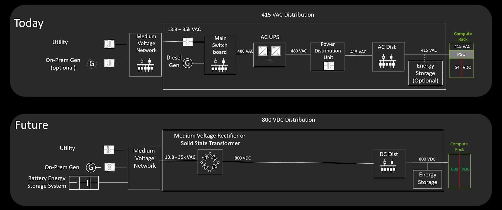
This reference architecture from NVIDIA for next generation data centre power infrastructure shows the reduced complexity from use of an SST, allowing for DC-only power at the rack level (Image credit: NVIDIA).
The common theme in these scenarios is smaller size and less waste heat, but there is another fundamental shift going on here as well. When power is shaped and controlled by passive devices, we need a wide array of different transformers and other devices to support scenarios where the input and output demands vary widely. Power electronics operate more like a router on a data network, chopping the power into small packets and then using software to control the flow to various outputs as needed. This makes them much better suited to the more dynamic power needs of modern applications like solar, wind, and batteries (whether of the EV or BESS variety).
Another key advantage of the fine-grained “power routing” abilities of an SST is their ability to handle bi-directional power flow. With the addition of grid-scale storage, power on many elements of the distribution grid need to handle energy flow both to and from the storage node. Roof-top solar adds a similar requirement on the distribution grid. The traditional passive grid infrastructure is not well suited to support this. Protection relays in the grid are typically directional, designed to trip only when they detect a fault flowing from the substation to the customer. Even tricker, the inversion of flow creates harmonic distortion in the electricity waves that can be amplified as they travel through the grid. A useful analogy is to think of the distortion of water when two ships travel in opposite directions and their wakes collide. Since an SST chops the power into discrete pulses of DC current, and then assembles a “fresh” AC current on the other end, it acts like a buffer that eliminates any harmonic distortion in the process. To stretch my water analogy, it lifts buckets of water out a turbulent river and pours them gently into a fresh new stream.
Adoption on the wider grid
Although SiC MOSFET devices today play a limited role on the edges of the grid, the usual semiconductor adoption curve is already clearly evident, with prices steadily falling and reliability maturing. This process really took off in 2018 when Tesla first used SiC MOSFET technology in the main power inverter of the Tesla 3. The device-level cost relative to silicon IGBT devices has fallen from a factor of 10x more expensive in 2020, to 3x today. This is already enough for total system cost parity in many applications thanks to reduced size and cooling requirements. Cost reductions were accelerated by a move from 100mm to 150mm wafers, allowing more chips per wafer and reducing fabrication costs. The next transition to 200mm wafers is already underway, and expected to yield similar cost savings (EE Power). The market is projected to expand rapidly over the next decade, as it moves into large scale applications such as distribution grid transformers (Grand View Research). On the reliability side, adoption in the automotive sector has proven their quality on a 10-year time scale, but there is more work required to prove they can handle the 25-40 year lifespan of grid components.
Power electronics on the grid tie together many of the topics I’ve covered in previous posts. They can be used to address the inertia problem, and they enable the shift to DC transmission. And of course they are essential for integrating any variable or flow-reversing technologies such as solar, wind, and battery storage. The ability to control power flows with software also allows for demand-response programs to reduce bottlenecks and maximize use of limited transmission infrastructure. The technology required to support power electronics at grid-scale voltage has been slow to mature, but is now hitting a crossover point where it is ready for wider adoption. While this kind of underlying power infrastructure is often overlooked, it is a key building block for the ongoing energy transition.
Resources
Introduction to Power Electronics - Lecture 1 from a full MIT course on power electronics. The subsequent lectures in this series require a strong background in math and linear circuits, but this first lecture is higher level and builds up a simple example power switch from first principles.
Power Electronics as an Enabler of the Current and Future Grid - National Laboratory of the Rockies (formerly NREL) presentation on power electronics for grids. Very technical detailed.
State of the SiC MOSFET - Very technically detailed, but a good overview of the history of SiC MOSFET devices
Why Grid Modernization Is No Longer Optional - Not much technical detail, but a good summary of the scenarios that are not well supported by traditional passive grid infrastructure.
Unleashing Unprecedented Performance - This is essentially marketing material from Wolfspeed, one of the pioneers of silicon carbide power electronics. However it gives a very clear and readable overview on silicon-carbide, its advantages, and use cases.
Smart Grids - High level overview of smart grid use cases, from the Canadian Climate Institute
Power Electronics: The Hero the Grid Needs - Long but very readable article on the importance of power electronics to the future electric grid, from the founder of Heron Power